


Analysis of PCB Double-Sided Board and Multi-Layer Board Manufacturing Processes and Key UV Ink Technologies
Abstract:
This paper delves into the manufacturing processes of PCB double-sided boards and multi-layer boards, and elaborates on the functions and selection criteria of core components such as various alkali-soluble photocurable resins, reactive diluents, and photoinitiators. It provides professional references for the optimization of PCB manufacturing processes and material selection.
In the previous article, we elaborated on the manufacturing procedures of single-sided printed circuit boards and related ink technologies. This article will continue with this theme, conducting an in-depth analysis of the manufacturing processes of double-sided boards and multi-layer boards as well as the composition of their supporting inks.
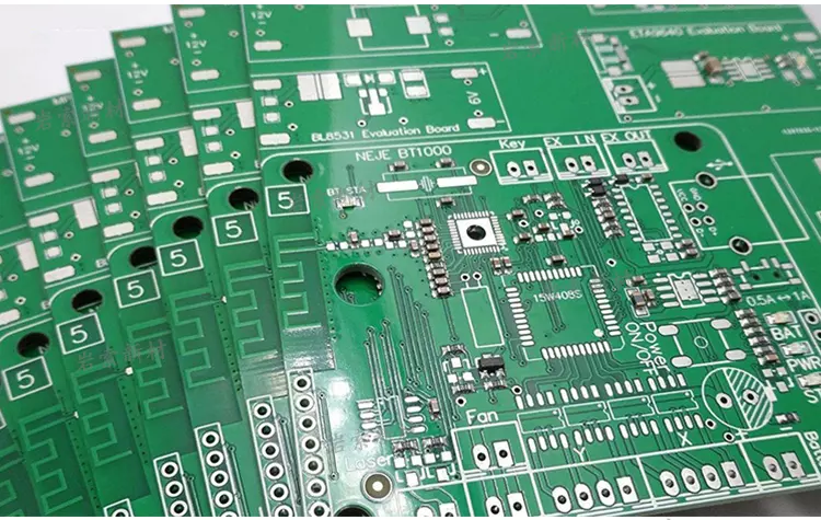
一、 Manufacturing Processes of Double-Sided Boards and Multi-Layer Boards
Double-sided boards and multi-layer boards mainly adopt the wet film process, with the core steps as follows:
✿ 1. Substrate treatment:
Pretreatment of copper-clad laminates
✿ 2. Pattern transfer:
Screen printing/roller coating/spraying of photoimageable anti-etching ink → pre-baking → UV exposure → development
✿ 3. Metal layer treatment:
Etching (or selective electroplating) → film stripping → drying
✿ 4. Solder mask protection:
Screen printing/curtain coating of photoimageable solder mask ink → pre-baking → UV exposure → development → post-curing
✿ 5. Identification printing:
Printing of UV character ink → UV curing
✿ 6. Quality inspection:
Finished product testing
This process relies on three key UV inks: photoimageable anti-etching ink, photoimageable solder mask ink, and UV character ink.
二、 Photoimageable Anti-etching Ink (Wet Film Technology)
As a core material for high-precision circuit pattern production, wet film can achieve higher resolution than dry film through direct contact exposure (without base film interference), making it the preferred technology for high-density PCBs.
Composition of Photoimageable Anti-etching Ink:
✿ 1. Alkali-soluble photocurable resin
✿ Novolac epoxy acrylate resin (low cost, good dimensional stability, mainstream choice)
✿ Epoxy acrylate resin composite (fast photocuring speed)
✿ Triphenol-based resin (excellent electroplating resistance)
✿ 2. Reactive diluents
The curing speed and film performance are adjusted through the compounding of mono-/di-/multi-functional monomers.
✿ 3. Photoinitiator system
The combination of potoinitiator 907 + ITX/651 enables efficient initiation, taking both deep curing and surface reaction into account.
✿ 4. Pigments, fillers, additives, etc.
二、 Photoimageable Solder Mask Ink
This ink protects non-soldering areas during wave soldering and provides a permanent insulating layer, with its technical key point being the adoption of a dual-curing system.
Composition of photoimageable solder mask ink:
✿ 1. Photocurable resin
Novolac epoxy acrylate resin is mainly used to ensure rapid UV forming.
✿ 2. Thermosetting resin
Multi-epoxy compounds (such as novolac epoxy resin) are combined with latent curing agents (imidazoles/dicyandiamide) to achieve high-temperature post-curing.
✿ 3. Reactive diluents
Enhancing hardness: TMPTA, PETA, etc.;
Improving flexibility: TPGDA, HDDA, etc.;
Reducing viscosity and increasing adhesion: (meth)acrylic hydroxyl esters, etc.
✿ 4. Photoinitiators
Multi-component combinations such as potoinitiator ITX/907/369/TPO/651, adapting to different curing requirements.
✿ 5. Functional additives
Phthalocyanine green, defoamers, adhesion promoters, etc.
This article systematically sorts out the technical logic and formulation design key points of ink materials in multi-layer PCB manufacturing. If you need support for specific raw materials or processes, please feel free to contact our technical team. We are committed to providing high-performance ink solutions for the industry and look forward to creating value with you!
(Note: For details on UV character ink technology, please refer to the previous text; it will not be repeated here.)